
The global energy crisis looms large as a major challenge facing humanity. To prevent potentially catastrophic environmental, economic and geopolitical consequences, green technologies are being championed for the energy-hungry industrial sectors of the economy. In the area of lighting, for instance, which currently consumes 20 percent of the world’s electricity, high-efficiency visible light-emitting diodes now provide a green alternative to incandescent and fluorescent lamps.
The Internet represents one of the fastest-growing energy gobblers in modern society. Internet transmission and switching equipment consume roughly 0.5 percent of the total electricity supply in developed countries, and that figure is expected to rise to 5 to 10 percent as the data rate in the access portion of the networks reaches 100 Mbps. Energy consumption is rising fast due to the insatiable demand for bandwidth.
Moreover, the electricity bill of mega data centers—which are the backbone of companies like Google—is currently 1.2 percent of global electricity consumption, half of which is consumed in information-technology equipment. These data centers are experiencing a very high annual growth rate of 16 percent worldwide, and they may consume 5 percent of the world’s electricity in a few years.
The fast-growing Internet traffic has indeed resulted in a dramatic increase in power consumption, since the heat dissipated in data centers is nearing 20 kW per square foot of area, with 28 percent annual growth for communication equipment as its main constituent. This trend is creating formidable economic and logistical challenges for Internet companies, as well as for utility companies that must meet their ever-increasing demand for electricity.
Meanwhile, to speed up communication links, electrical interconnects are being replaced with optical counterparts for shorter and shorter distances. The battle-line between metal and optical interconnects is currently at rack-to-rack communications—that is, the lengths within data centers. This line is moving closer to the chip, and we expect that optical interconnects will provide chip-to-chip communication and possibly even intra-chip communication in the future. Wherever the final boundary winds up, photonic components will undoubtedly become more widespread in computers and consumer electronics. Given that computing-related power usage accounts for 15 percent of the United States’ electricity consumption, the energy efficiency of photonic components will have paramount economic consequences.
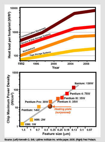 Heat load and power density. (Top) From 2000 to 2010, the annual rate of increase for heat density in data centers ranges from 7 to 28 percent for communications equipment. The vertical axis is plotted on a logarithmic scale, which highlights the alarming increase in power density. (Bottom) Similarly, there is a dramatic increase in the power density of VLSI chips. Consequently, photonic devices must be able to operate on the hot VLSI substrate and their own power dissipation must be minimal.
The need for energy-efficient photonics is exacerbated by the excessive energy dissipation in advanced electronics—the world to which photonics must adapt. As described by Moore’s law, transistor count has been increasing at an astonishing pace in today’s microprocessors. For instance, the Intel Itanium II chip boasts nearly 2 billion transistors. An unintended consequence is that the power density has already exceeded 100 W/cm2, which challenges even the most advanced chip-cooling technologies. This has important implications for photonic devices, for they must be able to operate reliably at substrate temperatures as high as 90° C. The problem of heat dissipation is so severe that it threatens to halt the continued advance of the industry. It has prompted the recent momentous shift of the microprocessor industry away from increasing clock speed and in favor of multi-core processors.
Silicon: an attractive platform for photonics
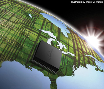
Silicon is becoming the material of choice for manufacturing photonic components that overcome the communications bottleneck in computing and telecommunications equipment. The prevailing vision for silicon photonics has been to integrate optics and electronics on the same chip. This approach makes sense considering the material and process compatibility between silicon photonics and the dominant microelectronics technology, known as the complementary metal-oxide-semiconductor (CMOS) process.
To uncover the challenges that lie ahead, we must evaluate the full implication of “compatibility.” Full compatibility consists of material, process, economic and heat considerations. Material and process compatibilities are self-explanatory and much easier to satisfy than economic and heat compatibilities. Economic compatibility dictates the highly efficient use of wafer real estate and products that have a high-volume market. Heat compatibility requires that photonic devices must be able to operate on the hot very-large-scale integrated (VLSI) chip and that their own power dissipation must be minimal.
Among photonic components, lasers and laser-driver circuits are the most power-hungry devices. To date, the lack of any viable electrically pumped silicon lasers dictates an architecture where the light source remains off-chip. This architecture is in fact preferred as it removes a main source of heat dissipation. Furthermore, the performance degradation of injection lasers at high temperatures may be an obstacle to their integration onto the “hot” VLSI substrate, even when such silicon lasers are demonstrated.
 The communications bottleneck imposed by metallic interconnects. Optical interconnects are thought to be one way to solve the interconnect bottleneck. However, for optical interconnects to replace their copper counterparts, they must be energy-efficient.
Modulators, amplifiers, photodetectors, and perhaps wavelength converters are destined to be integrated on-chip. Among these devices, the modulator and the amplifier have the highest power dissipation. Similar to bipolar transistors, carrier-injection-type optical modulators suffer from static power dissipation. On the other hand, depletion-mode free-carrier modulators, as well as devices based on the quantum-confined Stark effect in Si/Ge quantum wells, will have low static-power dissipation.
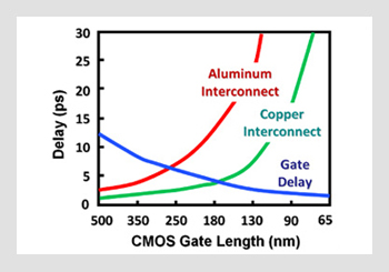
In addition, conventional wisdom holds that optical interconnects are much better suited than copper interconnects to handling high data rates (>10Gb/s). Hence, silicon photonics may be a solution for solving the communications bottleneck problem in CMOS VLSI electronics. However, with the use of equalization and other signal-processing techniques, copper interconnects can address higher and higher data rates, albeit at the cost of higher power dissipation. Therefore, for silicon optical interconnects to replace their copper counterparts, they must be more green.
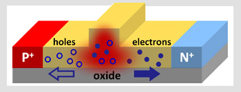 A silicon rib waveguide with a p-i-n junction diode.
Energy efficiency of silicon photonics
The amount of information that can be sent through an optical channel increases with optical power. Meanwhile, to address the real-estate economics of silicon wafer manufacturing, photonic devices must have footprints that are as small as possible. The concomitant reduction of a waveguide cross-section leads to an optical intensity that increases with data rate. Furthermore, in the absence of second-order optical nonlinearities, the operation of a wide range of silicon photonic devices, such as amplifier and wavelength converters, is based on third-order optical nonlinearities, such as Kerr and Raman effects.
However, high optical intensity is a prerequisite for the onset of the Kerr and Raman effects—an unfortunate situation that leads to a two-fold energy-dissipation crisis. First, optical power is converted to heat through two-photon absorption (TPA). Second, photons are lost not only because of TPA, but even more so by free-carrier absorption (FCA). The TPA-generated free carriers must be actively removed from the waveguide core; otherwise, they will accumulate, absorb the light and convert it into heat. While the problem can be mitigated by reducing the carrier lifetime (hence preventing the carriers from accumulating), processes that reduce the lifetime often result in higher optical losses.
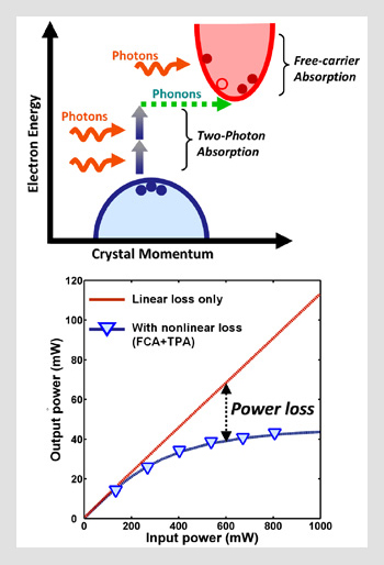 Nonlinear losses and optical power. Two-photon absorption (TPA) generates free carriers, which in turn cause a significant amount of free-carrier absorption (FCA). These nonlinear losses severely limit transmitted optical power. The loss of photons is the main problem facing a new class of silicon devices that exploit nonlinear optics to perform optical amplification, lasing, wavelength conversion and switching.
To date, carrier sweep-out using a reverse-biased p-n junction diode has been the only successful approach for dealing with the problem. However, this technique has its own issues: While it sweeps out the carriers and eliminates free carrier loss, the reverse-biased diode dissipates electrical power. As a case study, as much as 1 W of electrical power has been consumed in enabling the operation of early continuous-wave (CW) silicon Raman lasers that generated a few milliwatts of optical power. To put this into context, MOS transistors in electronics consume about a million times less power. Another energy-efficiency problem with the carrier sweep-out is that the optical power consumed to two-photon absorption is lost forever. Clearly, a more energy-efficient solution is needed.
Two-photon photovoltaic effect to the rescue
We have previously proposed and demonstrated a new carrier sweep-out technique that not only does not require electrical power dissipation but generates electrical power as well. The technique is based on our discovery of the two-photon photovoltaic (TPPV) effect, a useful effect that allows one to sweep the carriers away and eliminate the free-carrier absorption, while at the same time harvesting the energy of the photons lost to TPA. The key to understanding this function is that the prerequisite for carrier sweep-out is not reverse-diode voltage but rather reverse negative current.
Thus, if the p-n junction is biased in the fourth quadrant of its current voltage-transfer function, the TPA-generated carriers are swept out by the internal field of the junction (created by the difference in electron concentration between the n and p sides); yet the device has negative electrical power dissipation. In other words, it delivers power to an external load. This is because, under this operating condition, the product of the diode current and voltage and hence its power dissipation is negative. The source of the generated power is the photons that were lost to TPA. This novel photovoltaic effect can be perceived as the nonlinear equivalent of the conventional photovoltaic effect used in solar cells.
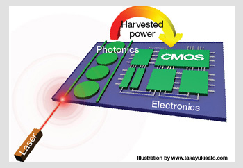 Energy harvesting through the two-photon photovoltaic effect can be utilized to supply the electrical power to electronics circuitry in optically interconnected VLSI chips.
We have applied this energy-harvesting technique to three types of key active devices—namely, optical amplifiers, wavelength converters and electro-optic modulators. The combination of very high data rates and small waveguide cross-sections results in high intensities in silicon optical interconnects. Thus, this energy-harvesting technique is, in principle, applicable to passive interconnects as well as active devices.
Normally, the severe TPA and FCA prevent CW operation of silicon Raman amplifiers. As a demonstration of energy harvesting in silicon optical amplifiers, we measured the Raman gain in silicon waveguides at different optical pump powers and electrical bias conditions of the diode. A CW gain of more than 6 dB is obtained at a reverse bias of 15 V, but at the cost of 150 mW electrical power dissipation. Raman gain of about 3 dB is measured when the device is biased to exploit the TPPV effect, resulting in electrical power generation (negative dissipation) of around 5 mW.
Researchers have also demonstrated energy harvesting and conversion-efficiency improvements in silicon wavelength converters. In addition, they have proposed an electro-optic modulator that takes advantage of the TPPV effect to attain negative static power dissipation. Clearly, TPPV offers an energy-efficient solution for nonlinear silicon photonics.
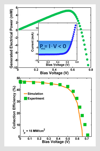 Electrical power generation and electron collection efficiency vs. voltage. (Top) The measured current-voltage behavior (inset) of a p-i-n diode shows the photovoltaic effect taking place in the fourth quadrant (Current < 0, Voltage > 0), where power dissipation is negative—i.e., where power generation is taking place. Electrical power as high as 5.5 mW can be harvested. (Bottom) The measured quantum efficiency of the two-photon photovoltaic effect at maximum power generation bias is within 39-41 percent, compared to the theoretical maximum of 50 percent.
Efficiency of the two-photon photovoltaic effect
Since the objective is not to absorb all the light, but rather to harvest the energy of the light that is absorbed by TPA, the proper definition of quantum efficiency, ηq, is the number of collected carriers per absorbed photon via TPA. As two photons are required for generating one electron-hole pair, the maximum quantum efficiency is 50 percent. An approximate expression for power efficiency at the voltage bias Vm that gives the maximum generated power is
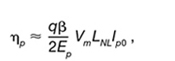 |
where q is the electron charge, β is the TPA coefficient (0.5 cm/GW at 1.55 µm wavelength for silicon), Ep is the photon energy and Ip0 denotes the coupled optical intensity at the input of the device. Also, LNL is the effective nonlinear length of the device; it takes into account the attenuation along the propagation, or z, direction:
 |
The TPA coefficient, β, and the optical intensity are the most important parameters that dictate the amount of optical power lost to TPA and hence the amount of electrical power generated by the TPPV effect. The TPA coefficient β is expected to be higher at shorter wavelengths—at 1.3 µm compared to 1.55 µm, for example, as has been observed experimentally in GaAs. In addition, FCA is lower at shorter wavelengths—which can increase the effective length. Therefore, the combination of the two effects will result in higher efficiency at shorter wavelengths.
Indeed, researchers have observed good agreement between analytical and experimental results. At lower pump intensities, quantum efficiency approaches the theoretical limit of 50 percent. The value of the efficiency at maximum power generation bias is about 40 percent, and is nearly independent of coupled optical intensity from 5 to 150 MW/cm2. Physically, this rather constant behavior occurs because the recombination current dominates the diffusion current at low biases and grows at approximately the same rate as the photogenerated current.
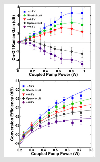 CW Raman gain and wavelength conversion efficiency vs. pump power. (Top) Measured CW Raman gain vs. coupled pump power in the waveguide with high reflectivity coated facets. (Bottom) Wavelength conversion efficiency as a function of coupled pump power under different biasing conditions in the same devices but without mirror coating. The wavelength detuning between the pump and the signal is 1 nm.
Future perspectives
The TPPV offers a viable solution for achieving energy-efficient silicon photonics devices. The effect reduces the optical loss by TPA and FCA, and serendipitously converts the optical energy lost to TPA to useful electrical power. The harvested power can thus be recycled to supply electrical power to electronics on the same platform. It is even possible to create a self-powered optoelectronic chip.
Beyond optical interconnects, another possible application of the TPPV effect is photovoltaic power converters (PPCs) and optically powered sensors for fiber-optic networks. PPCs are used for remote power delivery and are optimized for a wavelength range from 1,300 to 1,550 nm. PPCs that can provide a few mW to 100 mW power are commercially available.
The TPPV effect is ideal for delivering power to the sensors used for monitoring and managing fiber-optic networks. Such sensors typically measure the optical power at a given point along the fiber link. A silicon p-n junction waveguide operating as a two-photon photodetector has already been proposed as an in-line power monitor. Here, a small fraction of the signal is absorbed by TPA while most of the light is passed through. In this scenario, electrical power must be delivered to the monitoring point to provide the power needed by the photodetector and to drive the supporting electronic circuitry. With the TPPV effect, one may be able to construct a self-powered remote sensor that measures the optical power passing through the waveguide while at the same time providing power for the sensing circuitry.
The nonlinear photovoltaic effect is not limited to silicon; it is also applicable to compound semiconductors. Indeed, reported values of β at 1.3 µm in InP and GaAs are 70 and 42.5 cm/GW, respectively, versus 3.3 cm/GW in silicon, which is in turn more than six times higher than the aforementioned value of β at 1.55 µm in silicon. The FCA loss of III-V materials is typically the same as in silicon.
Hence, the TPPV effect is expected to have higher efficiency in compound semiconductors. This is important because researchers have recently reported that TPA and TPA-generated FCA can limit the output power of a high-power III-V-based semiconductor optical amplifier. Adding the TPPV effect to these devices may allow us to harvest the optical loss to electrical power and simultaneously to mitigate the TPA and the associated FCA optical loss through carrier sweep-out, as is the case in silicon. These advances will lead the way toward green integrated photonics that may have a profound effect on the telecom industry, the economy—and the health of the planet.
Bahram Jalali and Kevin Tsia are with the University of California, Los Angeles (UCLA), U.S.A. Sasan Fathpour was previously affiliated with UCLA, but is now with CREOL, the College of Optics and Photonics at the University of Central Florida, Fla., U.S.A.
References and Resources
>> J.G. Werthen. SPIE 2872, 1137 (1996).
>> D.A.B. Miller. J. Selected Topics in Quant. Electronics (2000).
>> K.G. Brill. White paper by Uptime Institute Inc. (2005).
>> B. Jalali and S. Fathpour. IEEE J. Lightwave Tech. 24, 4600 (2006).
>> Y. Liu et al. IEEE Phot. Tech. Lett. 18, 1882 (2006).
>> S. Fathpour and B. Jalali. Opt. Express 14, 10795 (2006).
>> K.K. Tsia et al. Opt. Express 14, 12327 (2006).
>> S. Fathpour et al. IEEE J. Quant. Electron. 43, 1211 (2007).
>> B. Jalali. Scientific American 296(2), 58 (Feb. 2007).
>> G. Lawton. Computer 40, 16 (2007).
>> M. Pickavet et al. BroadBand Europe Antwerp, Belgium (2007).
>> R. Tucker. IEEE Photo. Tech. Lett. 19, 2036 (2007).
>> A. Gladisch et al. Proc. ECOC 2008 Brussels, Belgium (2008).
>> P.W. Juodawlkis et al. Opt. Express 16, 12387 (2008).
>> R. Tucker et al. Proc. ECOC 2008 Brussels, Belgium (2008).
>> M. Webb. “SMART 2020: Enabling the low carbon economy in the information age,” A report by The Climate Group, Creative Commons (2008).