
 [Getty Images]
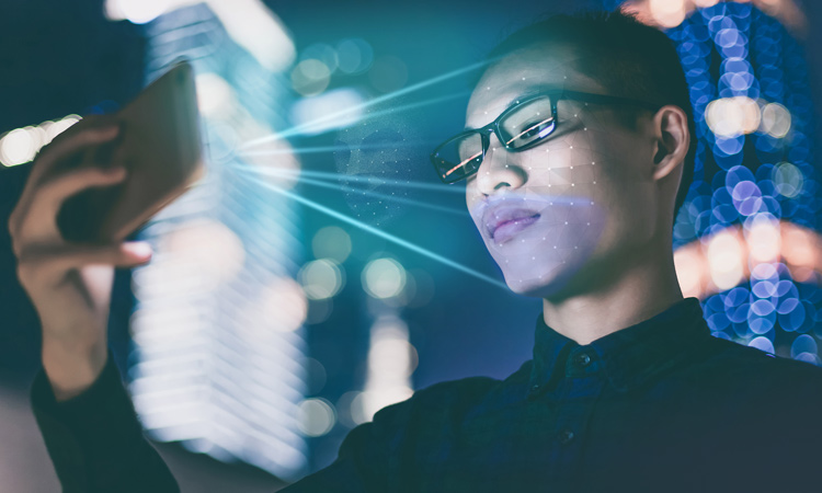
The November 2017 release of Apple’s iPhone X, with its “Face ID” authentication by facial recognition, highlighted the disruptive potential of 3-D sensing via mobile devices—a technology that could ultimately find use in hundreds of millions of smartphones worldwide. The sudden transition in 3-D sensing in mobile devices has stoked unprecedented demand, and a new market, for vertical-cavity surface-emitting lasers (VCSELs); and, more generally, for the GaAs/AlGaAs near-infrared semiconductor lasers at the heart of these systems. And while semiconductor edge-emitting lasers (EELs) already serve traditional industrial and telecom markets, their fastest future growth could come in 3-D sensing, with the lion’s share going toward mobile electronics.
Compact, efficient, and featuring narrow and stable linewidths (in contrast to the familiar LED light sources already embedded in smartphones), the current generation of GaAs/AlGaAs semiconductor lasers fit the needs of this burgeoning market, as well as other core areas such as autonomous-vehicle sensing. But which of these diode lasers are best suited for which job? In this article, we provide an overview of the key attributes of diode lasers deployed in today’s consumer devices and an update on their state-of-the-art capabilities. We also compare the design and performance differences of the different laser types, to clarify where next-generation diode technology should focus—and how these devices can best intercept the 3-D sensing ecosystem.
 [Illustration by Phil Saunders] [Enlarge image]
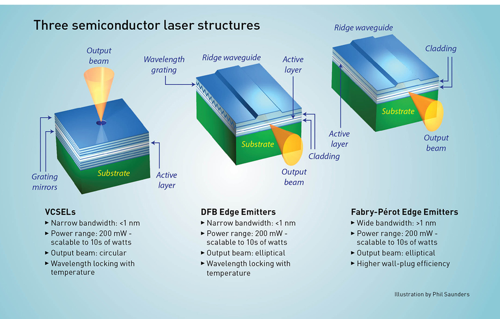
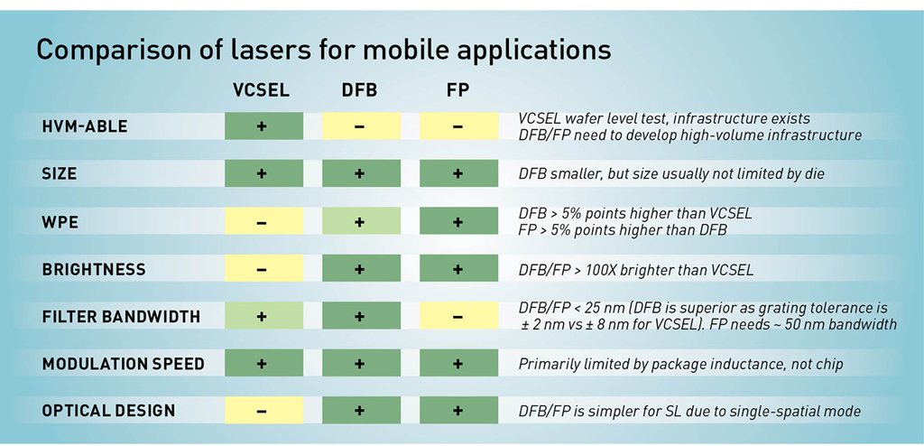
VCSELs and EELs
InGaAs/AlGaAs semiconductor lasers come in three types: VCSELs and two types of EELs. The VCSEL, as its name implies, emits vertically, normal to the plane of the device, owing to cavity mirrors grown within the epitaxial material itself. The VCSEL’s circular beam has a numerical aperture (NA) of roughly 0.2, or a full angle of approximately 25 degrees.
The importance of grating stabilization for VCSELs and DFB EELs becomes clear in the context of specific applications, such as the 3-D sensor on a smartphone.
By comparison, EELs have an elliptical emission with a similar NAx * NAy product, but with the beam exiting parallel to the device plane from a cleaved mirror. The two subtypes of EELs, distributed-feedback (DFB) EELs and Fabry-Pérot (FP) EELs, share most features in common, except that DFBs include a wavelength grating built into the structure, similar to VCSELs.
All semiconductor lasers require both electrical and optical confinement provided by sandwiching an active layer between materials of lower refractive index. For EELs, the carrier and lateral optical confinement can be achieved in several ways (for example, via a ridge waveguide) to reduce the effective refractive index. For VCSELs, oxidation of the epitaxial structure is the standard method for providing electrical and lateral optical confinement for data communications applications. Over the years, this method has been perfected and has proved extremely reliable and manufacturable.
One advantage that has led to VCSELs’ rapid adoption is that each emitter (or emitter array) can be fabricated and tested prior to wafer dicing. By comparison, EELs require cleaving followed by dielectric coating to form the mirrors before burn-in or testing. The ability to fabricate and test prior to wafer dicing offers an edge for consumer applications with huge volume ramps (potentially more than 100 million units per year), as it simplifies back-end assembly and capital demands.
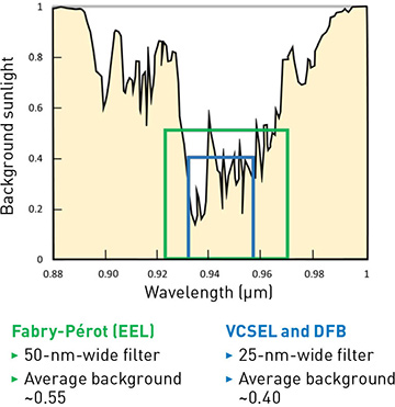 Competing with sunlight: Chart shows background sunlight transmitted through atmosphere versus wavelength; area enclosed by boxes represents the parasitic average sunlight that competes with the intended signal for semiconductor lasers in 3-D mobile sensing applications. Grating stabilization of VCSELs and DFBs allows substantially reduced linewidth and, thus, noise reaching the bandpass-filtered detector.
The narrow-linewidth advantage
An important factor for assessing these lasers for the 3-D mobile sensing market is the ability to operate outdoors, in sunlit conditions and in varying temperatures. Here, a key differentiator for both VCSELs and DFB EELs is a wavelength-specific grating built into the laser cavity, which forces lasing at only that specific wavelength. The grating also reduces the wavelength shift with temperature down to roughly 0.07 nm/°C—nearly an order of magnitude better than the nominal 0.3 nm/°C drift for a comparable FP EEL laser, which does not possess this grating element. (LEDs wavelength-shift with temperature and also suffer from linewidths greater than 150 nm, which limits their application in mobile devices to the camera flash.)
The importance of grating stabilization for VCSELs and DFB EELs becomes clear in the context of specific applications, such as the 3-D sensor on a smartphone. Moisture from the atmosphere absorbs sunlight in several wavelength bands, including the 940-nm range of greatest interest for these sensors. A bandpass filter mounted above the sensor reflects unwanted background light to improve the signal-to-noise ratio (SNR) for the sensor. The filter’s bandwidth must accommodate the entire wavelength variation, including the built-in wafer variation, wavelength drift over the entire temperature range, as well as the manufacturing wavelength tolerances of the dielectric filter.
For DFB EELs and VCSELs that are grating stabilized, both the built-in wafer variation and the wavelength drift with temperature are considerably lower than for FP diodes. Accordingly, the DFB and VCSEL can utilize a bandpass filter with a width of roughly 25 nm, while an FP laser requires a filter with around 50-nm bandwidth. That difference attenuates sunlight transmission from around 0.55 in the FP to 0.4 in the other laser types due to better overlap with the transmission minimum, providing additional noise reduction. (As a side note, the temperature-stability advantage for grating-stabilized lasers becomes even greater for applications related to the automotive market, where temperatures range from –40 to 125 °C, versus 0 to 70 °C for mobile environments.)
Initially, smartphone applications favored 830-to-850-nm diode illumination, due to the higher sensitivity of CMOS and CCD detectors at those wavelengths. However, atmospheric absorption of sunlight at 830–850 nm is much reduced, which degrades SNR. Due to the absence of Al in the active layer, 940-nm diodes provide higher reliable power that provides a sufficient offsetting benefit. Customers are thus migrating to the longer wavelength for both VCSELs and EELs, a trend that will likely continue.
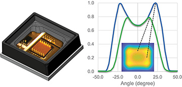 A ToF laser design: Left: Example design from Lumentum includes a uniform VCSEL array with split bond pads, photodetector for eye safety and a diffuser to homogenize and tailor the intensity profile over a specific FoV, in a package approximately 3×3×1 mm in size. Right: Angular intensity sliced along the center of both axes. The “winged” profile creates a flat-top distribution onto the detector, resulting in a more uniformly illuminated image.
The reliability of InGaAs/AlGaAs EELs has been long proven, since the first deployment of 980-nm EELs as pumps for optical amplifiers in submarine fiber cables. On the VCSEL side, initially there was concern that the design’s oxidized layers would generate stress and defects, degrading reliability. Years of wide-scale VCSEL deployments in short-haul data centers, however, have assuaged those fears. And with the recent proliferation of 3-D-sensing facial recognition in mobile phones, field deployment statistics collected from hundreds of millions of VCSEL arrays have corroborated their robustness.
Power, range and sensing architecture
The semiconductor laser best adapted for 3-D mobile sensing also hinges on the distance to be covered by the sensor, and the choice of 3-D sensing architecture for the job.
Whereas VCSEL emitters for data communications require powers of less than 10 mW, facial recognition takes several watts of peak power. To get there, several hundred individual VCSEL emitters can be fabricated to form a single array, with all emitters or sections of them electrically connected in parallel. A typical VCSEL array has a diode footprint of 0.5–1 mm2, including emitters and bond pads. Arbitrary patterns can be easily created lithographically to generate various locations and sizes of emitters and arrays. On the other hand, to achieve the same system-level performance, DFB chips are typically about half the size of the VCSEL-array dies, and need only one single-spatial-mode emitter to illuminate the diffractive optical elements (DOEs) to create the output pattern, which simplifies the optical design considerably.
Front-facing: range < 1m
The most successful technology for front-facing cameras, with application distances of less than 1 m, is “structured light,” in which a pattern of dots is illuminated onto subjects. (Another approach, “active stereo,” is a potential hybrid design that augments structured light with stereo vision.) An early example of a consumer 3-D sensor based on structured light was the system developed by Primesense for the Microsoft Kinect console, which used a single-mode Fabry-Pérot laser to illuminate multiple DOEs. More recently, a VCSEL array replaced the FP EEL diode. Both designs successfully eliminated the zeroth-order transmission, which is a nagging issue for eye safety.
World-facing (or rear-facing): range ~ 5 m
Next-generation, high-end phones will also include rear-facing 3-D sensing, with ranges up to around 5 m distance (for example, to detect and measure objects across a room). Longer distance requires significantly more power to achieve the same resolution, however, and the risks of eye safety become more vexing. One particular advantage of all EELs in these applications is their intrinsic emission brightness, which may help to extend the sensing range further.
Based on cost, size and performance tradeoffs, sensing for distances in this range, whether in mobile or other applications, may favor a different sensing architecture from structured light, “time-of-flight” (ToF) sensing. ToF modulates laser light from the VCSEL array source and compares the time delay between the outgoing and incoming optical pulses to calculate distance. The ToF architecture simplifies illumination requirements, as the diode array functions analogously to a monochromatic light bulb and the technical burden is redirected towards the detectors (for example, CMOS and CCD arrays) for resolution and sensitivity.
Pushing the envelope
In the rest of this article, we look at the state of the art for VCSEL arrays and DFB EELs for front- and rear-facing detection, and how engineers are pushing the specification limits of these devices. We focus on three particular challenge areas: e1fficiency, size and speed.
Challenge 1: Wall-plug efficiency
Wall-plug efficiency (WPE) simply equals the ratio of the light output power to total input electrical power. It dominates any discussion of future capabilities, because despite whatever technological path the industry chooses to embrace, greater performance and functionality from one’s mobile phone inevitably requires proportionally more output power that shortens battery life.
VCSELs feature WPE of slightly greater than 40 percent at nominal operating current at 60 °C; DFB EELs enjoy a lead of more than 5 percentage points above that. In addition, VCSEL efficiency falls off relatively faster at elevated temperature than does DFB efficiency. While mobile 3-D sensing thus far has included mainly front-facing applications of less than a meter’s range that might use a few watts of output power when energized, longer distances require higher powers for detection, as reflected power falls off as the square of distance—an obvious challenge for long-range sensing applications. Electrical driver power consumption also scales proportionally to diode current (and output power).
For facial-ID functions, deployment durations are short—perhaps less than an hour a day for the two to three year typical expected use of a smartphone, or around 1,000 hours of total “on” time. No one, however, can predict what sort of killer 3-D sensing app might spring into existence with substantially greater requirements. Finally, given greater power and more tightly spaced components, thermal crosstalk will put even more attention on improving WPE—not just for the diode lasers, but for other components that generate significant heat. All of these factors will put relentless pressure on development of diode lasers and other components to generate proportionally more power with less heat, regardless of the design and application.
Challenge 2: Reducing area
First-generation VCSEL diode arrays had an emitter spacing of some 20 to 30 μm with a typical emitter optical aperture of around 10 μm diameter. For structured-light and active-stereo applications, the pulse duration is typically greater than 1 ms, which approaches the thermal time constant of a VCSEL array—the duration at which the temperature rise saturates after change to the laser’s operating point. Wider emitter spacing mitigates thermal crosstalk and improves WPE. Designs for indirect ToF also suffer from thermal crosstalk, as the burst duration is also on the order of 1 ms and the duty factor of the burst may be as high as 50 percent.
With the ever-present trend of shrinking and compacting components for size and cost, improving WPE will be mandated for both VCSELs and DFBs.
These considerations matter, because improving resolution and shrinking dies to reduce cost inevitably requires reducing the emitter spacing and, once again, improving WPE. A typical structured-light system today consists of 10,000 to 30,000 dots illuminated onto a subject within a 60°×45° field of view (FoV) at up to 1 m distance. In a higher-resolution design that doubles the number of spots at the same FoV and distance, both the emitter aperture and spacing would need to shrink by some 40 percent. Even if WPE increased to offset the thermal crosstalk from tighter spacing, the optical crosstalk between adjacent emitters will have to be reduced by that same percentage.
Producing VCSEL arrays with optical apertures and NA with 40 percent better uniformity across a six-inch GaAs wafer, even with state-of-the-art processing equipment, represents a significant manufacturing challenge. Uniformity of emission is not an issue for EELs that utilize a single spatial mode, as the uniformity of diffracted spots is determined solely by the DOEs themselves. Accordingly, EELs have an advantage for higher resolution front-facing structured-light architectures.
Challenge 3: Speed
This last challenge relates to longer-range, ToF applications in particular—and to the output modulation speed bandwidth, which determines the depth resolution of these systems. VCSELs (or EELs) for these applications are modulated on-off at peak current and at frequencies greater than 100 MHz. Good pulse-edge resolution calls for a rise/fall time in the optical pulse of less than 0.3 ns—not a problem for VCSEL emitters in data communications, which operate at low currents. But present-day ToF designs require a few watts of power, or up to 3 amps of drive current.
Because any change in voltage is proportional to the change in current with time (dV = L dI/dt), the rise/fall time is proportional to the product of the inductance, L, and the drive current, dI. Therefore, to achieve shorter rise and fall times, low inductance, low drive current, or both are needed.
On the inductance side, a rise time of less than 0.3 ns at a drive current of 5 A essentially forces an inductance of less than 0.3 nH for a packaged diode laser. Although both VCSELs and EELs have an intrinsically small inductance, the electrical traces and wire bonds create a lower limit. To drive down inductance further, packages will need more electrical vias and wire bonds, and must keep the driver-to-diode spacing to an absolute minimum.
 [Getty Images]
Automotive demands
3-D sensors have a pivotal role for improving the safety of autonomous vehicles, as they provide real-time data about the physical environment, the vehicle and the driver, and allow 360-degree, comprehensive mapping of all objects surrounding the car, near and far.
Because of their higher efficiency and narrower bandwidth (and thus higher SNR), VCSEL arrays are actively targeted for replacing LEDs for in-cabin sensing (for example, to detect and warn a sleepy or texting driver). Short- to medium-range lidar is needed for blind-spot detection, lane-departure and rear-collision warnings. In this range, VCSEL arrays appear to be attractive candidates that can include emitter redundancy to allow a soft-failure mode that extends their lifetime.
Notably, automotive standards, such as the AEC-Q102 standard of the Automotive Electronics Council, will dictate more stringent requirements for operating-
temperature range (from –40 °C to 125 °C), qualification and reliability than for mobile 3-D sensing. In-cabin applications will require peak power greater than 10 W, and short-range lidar (covering less than 50 m) may require up to hundreds of watts in the future.
At such high optical powers, as with mobile 3-D applications, the migration to VCSELs designed for lower current at higher voltage seems inevitable in the long run. Similarly, more aggressive packaging requirements (such as flip chip) will need to be investigated to mitigate inductance.
 In the sensor-equipped cars of the future, VCSELs can be used to displace LEDs for in-cabin monitoring, and both VCSELs and EELs can be used for short- to medium-range detection—for example, rear-collision, blind-spot, and cross-traffic monitoring (green areas in diagram above).
For even faster rise/fall times or higher peak currents, the next-generation designs will require that the diode laser and drivers be co-packaged. Next-gen VCSEL arrays can further mitigate inductance by creating vias in the VCSEL substrate to eliminate wire bonds altogether.
Rather than focusing on inductance to reduce rise/fall time, engineers might also seek to reduce the peak drive current while operating at the same illumination power. Of course, this raises new technical challenges, such as greater manufacturing complexity or creating more complicated structures while still demonstrating the same high reliability of the ubiquitous single-junction semiconductor lasers so widely deployed over the past two decades.
A bright future
As the discussion above suggests, the three main types of semiconductor diode lasers—VCSELs and DFB and FP EELs—differ in their details in important ways. Both VCSELs and DFBs have a considerable advantage over FP lasers at 940 nm due to wavelength stabilization for outdoor use, and therefore will be popular choices for mobile 3-D sensing (as well as for emerging applications in the automotive market). Individually, VCSEL and DFB lasers have their strengths and weaknesses, depending on the specifics of the 3-D sensing architecture under consideration. With the ever-present trend of shrinking and compacting components for size and cost, improving WPE will be mandated for both VCSELs and DFBs.
Some of the advantages of VCSEL arrays—testable at wafer-level, narrow wavelength range, small size, high reliability—allowed them to catch the first wave of 3-D sensing applications. For world-facing 3-D sensing applications in particular, including automotive, the extreme power/current requirements will lead to more aggressive chip innovations compared with the front-facing applications now emerging in mobile phones. Notably, VCSELs and EELs will be transformed in order to increase modulation speed for higher resolution. DFB EELs appear positioned for a comeback in the mobile space, owing to their superior brightness and better WPE relative to VCSEL arrays and their narrow wavelength range relative to FP diodes.
While we’ve looked here at mobile 3-D sensing in particular, advances in these lasers will pave the way for new opportunities beyond that market. As the cost, reliability and uniformity of VCSELs and EELs reach or exceed parity with conventional light sources, diode lasers will eventually displace existing industrial technologies; heat lamps used for thermal annealing or conventional lasers for high-end printers represent such opportunities. These lasers thus face an exciting future—whether on the factory floor, in the car or in the palm of your hand.
Jay Skidmore is vice president of research and development with Lumentum, Milpitas, Calif., USA.